The LENA Nanometrology Center is equipped with a unique combination of high-end nanoanalytical instruments. High-resolution imaging techniques, spatially and temporally resolved spectroscopy, surface manipulation and analytics as well as devices for the measurement of particle properties are operated by the expert groups of the LENA.
The following large devices are part of the basic equipment of the LENA research building:
The micro particle image velocimetry (µPIV) method is based upon particle trajectories gained by two pictures taken at a short time interval (~500 ns). By the different particle positions in the images a velocity vector is calculated for each visible particle. Using all obtained velocity vectors the flow profile inside a micro- or nanochannel can be calculated. The results can be used to validate or replace simulations in difficult geometries. In addition to a 2-dimensional setup using one camera, stereoscopic measurements need two individual cameras for each picture in order to obtain a three-dimensional flow velocity profile.
The instrument will allow 3D particle velocity measurements using two cameras (3D2C-setup). The “stereo-micro-PIV FlowMaster” system consists of a Zeiss V20 stereoscopic apochromatic microscope with binocular phototubes equipped with two CMOS cameras. In addition a phantom high speed camera is available for high-pressure microsystems. The whole setup is placed upon a passively dampened optical table. As light source either a white LED illumination or a Nd:YAG double-pulse laser (type Nitron-Bernoulli) at 532 nm will be available. The software includes modules to test and determine 2-and 3-dimensional PIV, 3-dimensional strain and laser induced fluorescence (LIF).
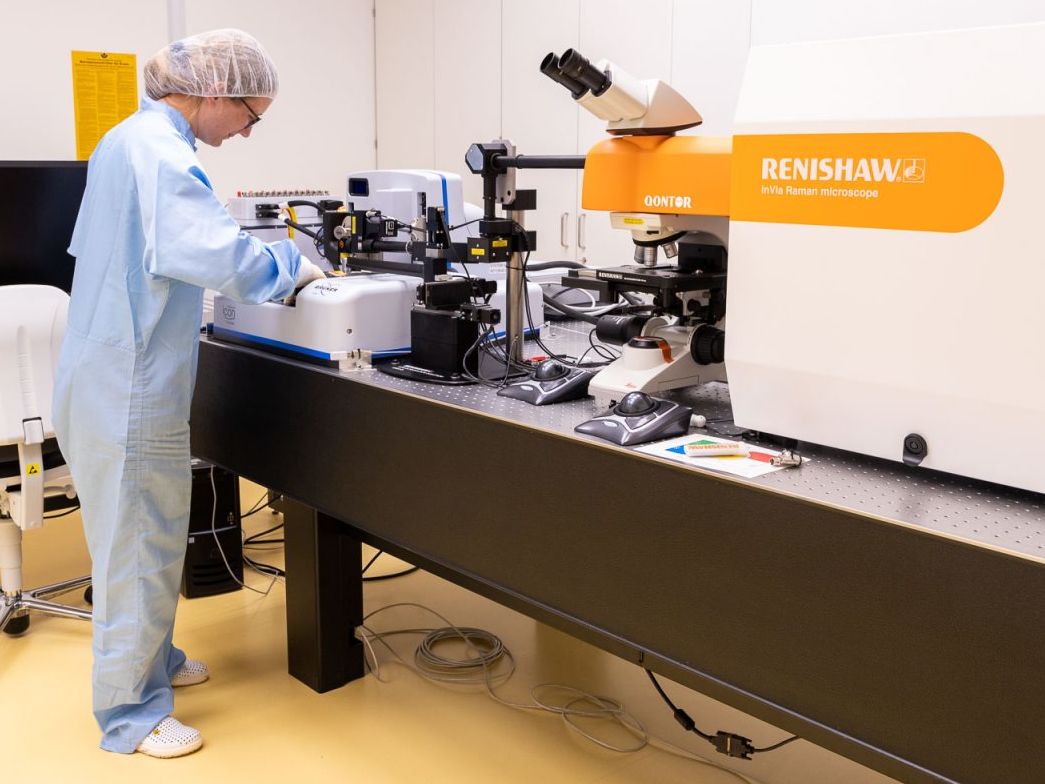
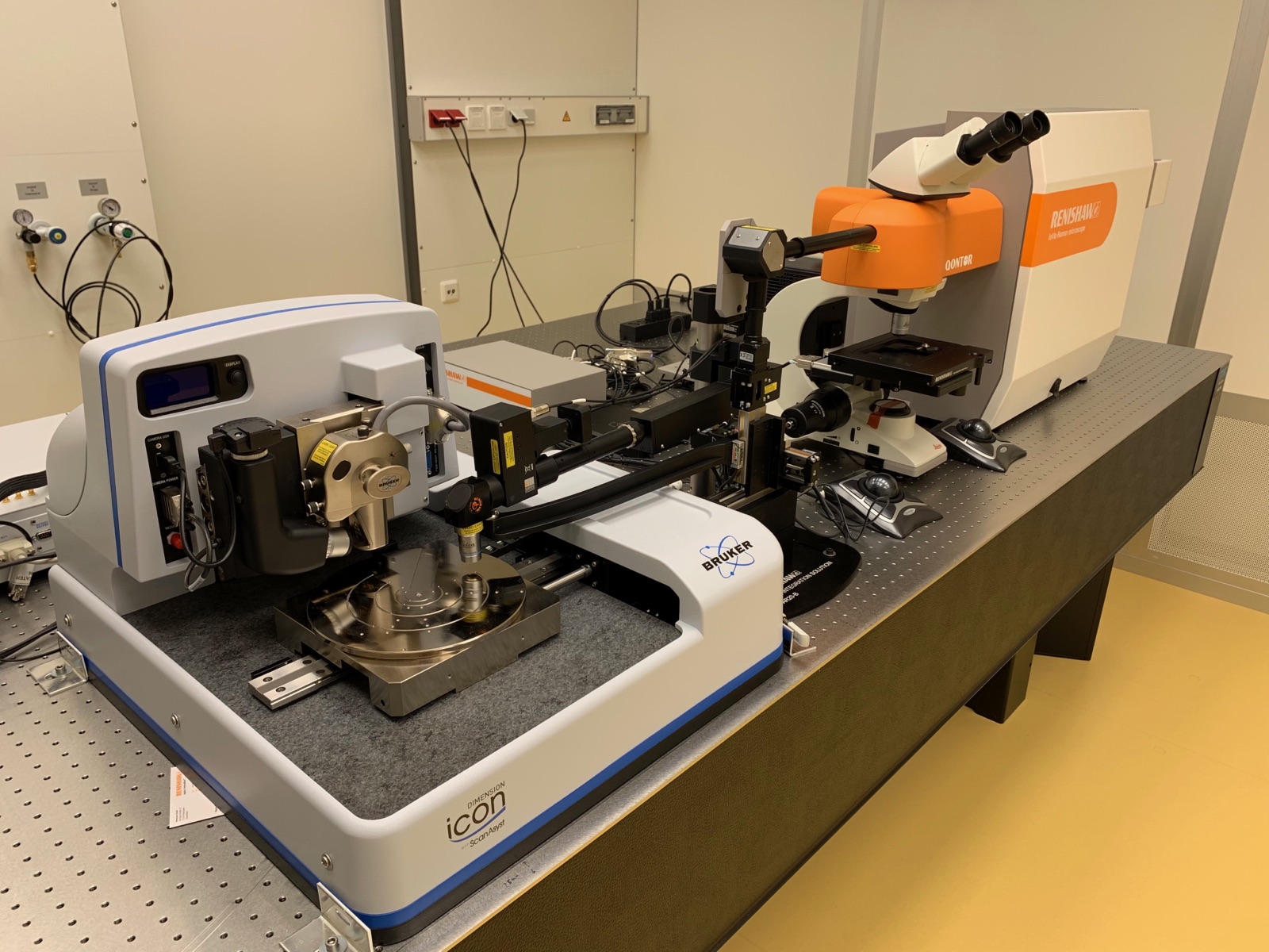
In the setup presented, a Bruker Dimension Icon Atomic Force Microscope and a Renishaw inVia confocal Raman Microscope are coupled together by a flexible arm.
This setup enables correlative microscopic measurements. For example, the topography and chemical composition of a sample can be determined in spatial resolution simultaneously.
The Atomic Force Microscope has an interface for the user to upgrade a 3D functionality, which also allows topographic measurements of the side profiles of three-dimensional structures to be recorded in a traceable manner1,2. The setup is currently taking place in strong collaboration with the PTB.
[1] G. Dai et al., Measurements of CD and sidewall profile of EUV photomask structures using CD-AFM and tilting-AFM, 2014 Meas.Sci.Technol. 25 044002, DOI: 10.1088/0957-0233/25/4/044002 [2] G. Dai et al., New developments at Physikalisch Technische Bundesanstalt in three- dimensional atomic force microscopy with tapping and torsion atomic force microscopy mode and vector approach probing strategy, 2012 Journal of Micro/ Nanolithography, MEMS, and MOEMS. DOI:10.1117/1.JMM.11.1.011004
The high resolution, double aberration corrected transmission electron microscope (JEOL Neoarm 200F) allows imaging nanostructures and thin films with atomic resolution. This system offers both the conventional transmission electron microscopy mode with parallel beam illumination (TEM) as well as scanning with a converged electron beam (STEM). Spherical aberration correctors as well as correctors for astigmatism up to 6th order for both TEM and STEM mode are built in. The specified spatial resolution is below80 pm. A cold FEG is used as electron source. The TEM samples can for example be prepared using our FIB to cut out lamellas from bulk samples. The double aberration corrected TEM is equipped with a number of different detector which allows for a manifold of investigation. These include bright field, annular bright field, and segmented high angle annular dark field detectors, as well as a backscattered electron detector. Besides spatial imaging and local diffraction, we can study the energy loss of the transmitted electrons (EELS) with an energy resolution below 0.3 eV. In addition, x-rays emitted due to excitations of atomic shell transitions by the transmitting electrons can be detected with spectral resolution (EDX) within a solid angle of 0.8 sr. This gives us the possibilities to study excitations or chemical composition of the investigated systems. Both EELS as well as EDX are possible in STEM mode which allows spatial mapping.
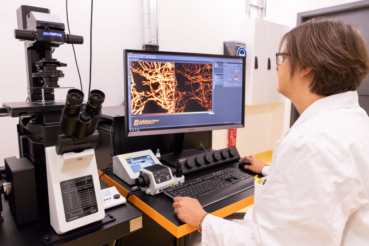
The inverse STED microscope from Abberior Instruments can be used for recording supperresolved fluorescence images with a resolution of 30 nm or better (depending on the sample).
The STED-wavelength is 775 nm (high-power-laser with > 2700 mW @ 40 MHz), excitation wavelengths are 561 nm and 640 nm. Suitable fluoresencce dyes include Atto647N, Abberior Star RED, Abberior STAR580 (for 2color imaging) as well as the fluorescent protein mCherry. Alternatively, protein labels like SNAP- and Halo-Tags can be used for live-cell-imaging.
The microscope includes a 2-channel detector unit, a FLIM-unit, a spectral detection module as well as different approaches for reducing phototoxicity and -bleaching (RESCue, DyMN und MINFIELD).
The Cryo-BLS system is an optical characterization platform for studying spin-wave dynamics and collective excitations in magnetic materials, superconductors, and hybrid quantum systems. The combination of Brillouin light scattering spectroscopy, micro-focused optical microscopy, and cryogenic operation enables spatially, temporally, spectrally, and phase-resolved investigations of low-energy excitations in functional materials and hybrid quantum devices.
The Cryo-BLS system was acquired through the DFG Major Research Instrumentation Programme (Art. 91b GG) under INST 188/590 (Project No. 567186839) and is operated by the Cryogenic Quantum Electronics Division at the Institute for Electrical Measurement Science and Fundamental Electrical Engineering (EMG). The system supports research in spintronics, magnonics, superconducting electronics, and quantum technologies. Typical applications include studies of spin-wave propagation, hybrid magnon-superconductor systems, and collective excitations in quantum materials.
The setup comprises a multi-pass tandem Fabry–Pérot interferometer, micro-focused BLS optics with 473 nm and 532 nm laser excitation, phase-resolved detection, and a closed-cycle helium cryocooler, an optical cryostat, and a positioning system. The setup provides optical access with sub-micrometre spatial resolution, operates over a temperature range from 5 K to 300 K, supports frequencies from DC to 20 GHz, and enables the application of in-plane magnetic fields up to 200 mT.
The MPMS-3 from Quantum Design is a SQUID-based magnetometer, which allows the highly sensitive measurement of the magnetic moment of solid and liquid samples in the temperature range from 1.8 K to 400 K in magnetic fields up to 7 T. The instrument is equipped with a closed-cycle cryostat and allows measurement in dc extraction as well as in vibrating sample mode (VSM). The latter allows measurements of magnetic moments < 10-11 Am2 in magnetic fields 250 mT. Complete hysteresis loops can be recorded in less than 1 h, depending on the magnitude of the magnetic moment. The MPMS-3 is additionally equipped with the AC option, which allows measurements of the complex magnetic susceptibility in the frequency range 0.1 Hz – 1 kHz at AC field amplitudes up to 1 mT.
The system allows the characterization of diluted samples of magnetic nanoparticles (both as suspensions, i.e. in the liquid state, as well as in the freeze-dried state) and of various thin-film samples with layer thicknesses down to 1 nm at a layer area of 5x5 mm2 and a magnetization of µ0M = 500 mT. The measuring system allows the investigation of samples with smallest magnetic moments as well as materials with large volumes and very large magnetic moments. For measurements of very small magnetic moments, the MPMS-3 is to be extended in perspective with the option of carrying out measurements in very small background fields.
Fieldemission scanning electron microscope Quattro S manufactured by FEI
Cathodoluminescence system SPARC manufactured by Delmic
Streak camera StreakScope S-20 manufactured by Hamamatsu
With the new cathodoluminescence measurement system, nanostructures can be investigated with high spatial resolution (Δx<50 nm), and time resolution (Δt<100 ps). Cathodoluminescence is based on the generation of electron-hole-pairs and their radiative recombination as a result of excitation with an electron beam. Time-resolution on a sub-nanosecond time scale is achieved by use of a pulsed electron beam. The recombination kinetics of the electron-hole-pails generates photons, which can be analyzed with the detector of the steak camera. From the emission spectra, e.g. information about the material composition, the electric structure and defects can be determined.
The measurement system consists of a scanning electron microscope Quattro S (FEI). A Schottky field emission cathode is used to generate the electron beam, whereby a spatial resolution of less the 50 nm is achieved. By deflecting the electron beam, electron pulses as short as 100 ps can be generated. Future research projects will reduce the time resolution to less than 10 ps.
The emitted light is detected by the SPARC-System (Delmic). Pan- and monochromatic spectra can be detected in a wavelength range from 200 nm (middle UV range) to 1000 nm (infrared range).
Time-resolved signals are detected using the streak camera StreakScope S-20 of Hamamatsu. Incident photons hit a photocathode and generate electrons. These are deflected by a time-dependent electric field before they hit a detector.
The measuring system is equipped with a cryostat to reduce the temperature of the sample down to 4 K.
This measurement setup for time-resolved femtosecond optical spectroscopy makes temperature- and power-dependent measurements of optical properties and charge carrier dynamics in nanostructures on different timescales (fs-ms) with high spatial resolution possible.
For the excitation a femtosecond Ti:sapphire laser system with nonlinear converters for wavelengths between 200nm and 2.5µm is used. The photoluminescence detection is realized by a streak camera with preceding spectrometer. This system covers the spectral range between 200 and 900nm with a temporal resolution of up to 1ps. The samples are mounted in a continuous flow helium cryostat and can be measured in reflection, transmission or confocal geometry at temperatures between 3.5K and 500K. Furthermore, an optical delay line for pump-probe experiments is available.
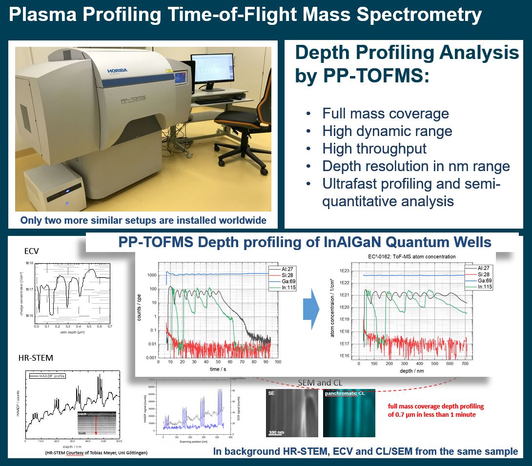
Plasma-profiling Time-of-Flight Mass Spectrometer (PP-TOFMS) from Horiba
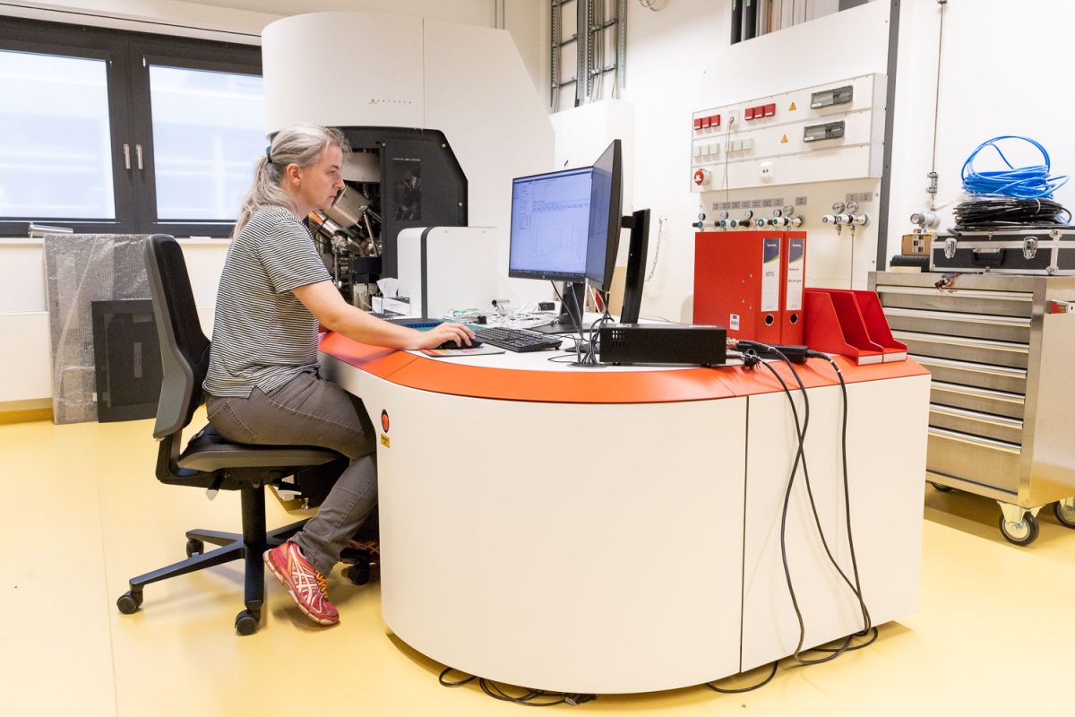
The device is a universal depth profiling tool that enables precise Time-of-Flight mass spectrometry (TOF MS) measurements of thin film structures with high throughput. This includes the precise determination of the composition of materials with a high depth resolution in the nm range. The depth profiling is achieved by forming a crater by plasma etching on the surface of the sample and then etching it vertically layer by layer and analyzing the formed ions by TOF MS. The required high sputtering rate is realized by the high ion density of the glow discharge plasma. The device ensures TOF mass spectrometry measurements on inorganic materials. Application examples include the analysis of dopants in semiconductors (incorporation behavior of dopants, diffusion), the detection and identification of surface contaminants. The device has a high level of availability as it is one of the key facilities at the new LENA research center, which will be used in parallel by several groups in physics, electrical engineering and chemistry.
The Crossbeam Focused Ion Beam (FIB) allows to create nanostructures by Ga-ion etching. The process can be controlled by a separate electron microscope (SEM). This allows a very versatile use. This system is in particular optimized to cut out TEM lamellas in essentially arbitrary geometry and transfer them to a sample holder for TEM measurements. The Ion beam energies can be varied from 500 eV-30 keV with a high energy resolution provided by a flight energy corrector. The spatial resolution is 4 nm at 30 kV (2,5 nm using selective edge mode) and 500 nm at 500 eV. The system also has a number of characterization possibility using the electron beam. The electrons are emitted from a Schottky Field effect cathode and the electron beam energies can be varied from 20 eV – 30 keV. Secondary Ion and electron detectors allow the use as Scanning Electron/Ion Microscope. In addition, the Scanning electron beam can be used in transmission in a STEM mode. Bright field dark field and high angle annular dark field detectors are available. The STEM resolution is 0.6nm @2kV and 1 nm @ 500V. The electron beam can also be used for electron beam lithography.
The sample stage allows very flexible operations and has a 150 mm travel in x and y (10 mm in z) and a tilt angle of 70°. An in-situ plasma cleaner is integrated.
Das Labor des Terahertz-Mikroskops mit seinen Vakuum-, Laser-, Hochfrequenz- und diversen anderen Systemen
The THz microscope uses a superconducting sensor, the so-called Josephson cantilever, to measure high-frequency radiation up to the terahertz range. The sensor can be moved very precisely in three dimensions by a high-resolution positioning system to also measure spatial radiation distributions. Active high-frequency circuits, such as radar chips or fast computer chips, can be investigated, as well as passive circuits that can be operated up to 40 GHz using a high-frequency generator or up to 7.5 THz using a far-infrared laser system.
The sensor is cooled to about 20 K by a pulse tube cryocooler. A second pulse tube cryocooler can be used to cool samples under investigation to temperatures as low as 4 K. The measuring chamber consists of a 55 x 50 x 50 cm³ shielded vacuum chamber. In addition to many electrical feedthroughs, the far-infrared laser can be quasi-optically coupled into the measuring chamber via another vacuum chamber containing optical setups. The entire setup is located on an actively damped optical table. The extensive measurement electronics in combination with the custom developed software allows many different measurement scenarios, often in cooperation with other groups. We welcome inquiries with ideas for joint measurements.

![[Translate to English:]](/fileadmin/_processed_/7/d/csm_XPS-02_1200x800_775b3e595f.jpg "[Translate to English:]")