Technische Universität Braunschweig
  • Study & Teaching
    • Beginning your Studies
      • Prospective Students
      • Degree Programmes
      • Application
      • Fit4TU
      • Why Braunschweig?
    • During your Studies
      • Fresher's Hub
      • Term Dates
      • Courses
      • Practical Information
      • Beratungsnavi
      • Additional Qualifications
      • Financing and Costs
      • Special Circumstances
      • Health and Well-being
      • Campus life
    • At the End of your Studies
      • Discontinuation and Credentials Certification
      • After graduation
      • Alumni
    • For Teaching Staff
      • Strategy, Offers and Information
      • Learning Management System Stud.IP
    • Contact
      • Study Service Centre
      • Academic Advice Service
      • Student Office
      • Career Service
  • Research
    • Research Profile
      • Core Research Areas
      • Clusters of Excellence at TU Braunschweig
      • Research Projects
      • Research Centres
      • Professors‘ Research Profiles
    • Early Career Researchers
      • Support in the early stages of an academic career
      • PhD-Students
      • Postdocs
      • Junior research group leaders
      • Junior Professorship and Tenure-Track
      • Habilitation
      • Service Offers for Scientists
    • Research Data & Transparency
      • Transparency in Research
      • Research Data
      • Open Access Strategy
      • Digital Research Announcement
    • Research Funding
      • Research Funding Network
      • Research funding
    • Contact
      • Research Services
      • Academy for Graduates
  • International
    • International Students
      • Why Braunschweig?
      • Degree seeking students
      • Exchange Studies
      • TU Braunschweig Summer School
      • Refugees
      • International Student Support
      • International Career Service
    • Going Abroad
      • Studying abroad
      • Internships abroad
      • Teaching and research abroad
      • Working abroad
    • International Researchers
      • Welcome Support for International Researchers
      • Service for Host Institutes
    • Language and intercultural competence training
      • Learning German
      • Learning Foreign Languages
      • Intercultural Communication
    • International Profile
      • Internationalisation
      • International Cooperations
      • Strategic partnerships
      • International networks
    • International House
      • About us
      • Contact & Office Hours
      • News and Events
      • International Days
      • 5th Student Conference: Internationalisation of Higher Education
      • Newsletter, Podcast & Videos
      • Job Advertisements
  • TU Braunschweig
    • Our Profile
      • Aims & Values
      • Regulations and Guidelines
      • Alliances & Partners
      • The University Development Initiative 2030
      • Facts & Figures
      • Our History
    • Career
      • Working at TU Braunschweig
      • Vacancies
    • Economy & Business
      • Entrepreneurship
      • Friends & Supporters
    • General Public
      • Check-in for Students
      • CampusXperience
      • The Student House
      • Access to the University Library
    • Media Services
      • Communications and Press Service
      • Services for media
      • Film and photo permits
      • Advices for scientists
      • Topics and stories
    • Contact
      • General Contact
      • Getting here
  • Organisation
    • Presidency & Administration
      • Executive Board
      • Designated Offices
      • Administration
      • Committees
    • Faculties
      • Carl-Friedrich-Gauß-Fakultät
      • Faculty of Life Sciences
      • Faculty of Architecture, Civil Engineering and Environmental Sciences
      • Faculty of Mechanical Engineering
      • Faculty of Electrical Engineering, Information Technology, Physics
      • Faculty of Humanities and Education
    • Institutes
      • Institutes from A to Z
    • Facilities
      • University Library
      • Gauß-IT-Zentrum
      • Professional and Personnel Development
      • International House
      • The Project House of the TU Braunschweig
      • Transfer Service
      • University Sports Center
      • Facilities from A to Z
    • Equal Opportunity Office
      • Equal Opportunity Office
      • Family
      • Diversity for Students
  • Search
  • Quicklinks
    • People Search
    • Webmail
    • cloud.TU Braunschweig
    • Messenger
    • Cafeteria
    • Courses
    • Stud.IP
    • Library Catalogue
    • IT Services
    • Information Portal (employees)
    • Link Collection
    • DE
    • EN
    • Instagram
    • YouTube
    • LinkedIn
    • Mastodon
    • Bluesky
Menu
  • Organisation
  • Faculties
  • Faculty of Electrical Engineering, Information Technology, Physics
  • Institutes
  • Institute of Semiconductor Technology
  • Research
Logo Institut für Halbleitertechnik der TU Braunschweig
Nitride Technology Center
  • Research
    • Nitride Technology Center
    • MicroPhotonicsLab (MPL)
    • Nano analytic
    • 2D materials
    • MEMS
    • DNA Origami & Molecular Electronics
    • Optical quantum technologies
    • Inverse Photonic Design
    • Cavity Optomechanics
    • Publications
    • QUANTista

Nitride Technology Center

Fotos von allen Projektleitern innerhalb des NTC

The Nitride Technology Centre (NTC) is shaping the rise of nitride technologies such as micro-LEDs as the second pillar of microelectronics. A central component here is to realise the sustainability potential of nitride technology – high luminosity with low power consumption. Furthermore, GaN components should be brought together with conventional silicon microelectronics in order to combine performance and innovative strength and thereby open up completely new fields of application. The NTC operates interdisciplinary projects with a focus on the integration of nitride and silicon technology and their applications in, for example, optical neuromorphic networks for the artificial intelligence of tomorrow.
With Braunschweig's pioneering role in the research of micro-LED technology, the NTC is a driving force for start-ups, SMEs and joint technology development. In addition to research and application, the NTC educates a specialized microelectronics workforce for tomorrow.

News

19.05.2025

Measuring quantum chips

10.04.2025

What’s going on in the quantum year in Lower Saxony?

28.02.2025

The spaceship among converters

19.12.2024

Roadmap for quantum careers around the world

05.12.2024

Professor Stefanie Kroker receives ERC Consolidator grant

26.11.2024

CMOS chips at the cold limit

25.11.2024

Micro-LEDs for neuromorphic computing

22.11.2024

Niedersachsen Science Prize in three categories for TU Braunschweig

more
Epitaxy

Within the last 30 years, the group III nitride semiconductors (GaxAlyIn1-x-yN) revolutionised the optoelectronics. Based on the p-doping, which was shown 1989, the first efficient blue light emitting diode (LED) was presented in 1992 and the blue laser diode followed in 1997. These developments were honoured with the Nobel Prize in Physics in 2014. The lighting technology, the main area of application, will have an estimated market volume of 64 billion US$ in the year 2020.

The development of group III nitrides was possible only due to the technology of metalorganic vapour phase epitaxy (MOVPE). This growth method is used for almost all commercial group III nitride devices today.

In MOVPE hydrides (e.g. ammonia) and metal organic precursors (e.g. trimethylgallium) are transported into a reactor, partly by means of a carrier gas. In the reactor the susceptor, which is carrying the monocrystalline substrates (wafers), is heated to temperatures of around 1100 °C. Under these high temperatures the molecules of the precursors are party cracking. Ga and N are forming crystalline GaN on the wafer surface while the residual molecules and the carrier gas are pumped out of the reactor and filtered in a scrubber. For a successful MOVPE process it is very crucial to work under highest purity (no impurities from precursors or reactor leakages) and to have a precise control over the process parameters (like e.g. temperature, pressure and gas flows) and thereby over the properties of the growing semiconductor layers.

Two MOVPE setups for group III nitrides are in use at the Institute of Semiconductor Technology. GaN, InGaN and AlGaN layers can be grown as crystalline layers with controlled thicknesses and doping concentrations. Based on this expertise, application-specific layer stacks are designed and manufactured. In a next step these crystalline layers are characterised (e.g. by XRD, SEM, AFM, CL, PL or TEM, see Nano Analytic) and processed (see Processing/Deep Etching) depending on the specific application.

Besides the growth of planar layer stacks we are also developing the epitaxy of three-dimensional architectures. These are manufactured by selective area epitaxy: A template (e.g. a wafer with a GaN buffer layer) is party covered by a structured SiOx mask. Under special epitaxy conditions, walls of GaN (so-called fins) can be grown in line-shaped openings of the mask. These fins feature non-polar sidewalls with low defect densities which could enhance the efficiency of LEDs drastically. We are investigating Fin LEDs for the visible (InGaN/GaN) as well as for the ultraviolet (AlGaN/GaN) spectral range.

Contact: Jana Hartmann

Foto von MOVPE Anlage und von Reaktor
SEM Abbildung und hyperspektrales CL Mapping eines GaN Fins mit AlGaN Mantelschichten im Querschnitt
SEM and hyperspectral CL of GaN/AlGaN Fin
Sputtering

The market volume of gallium nitride (GaN) based semiconductor technologies is estimated to 64 billion US$ for 2020 and is mainly enabled by use of the metalorganic vapour phase epitaxy (MOVPE). On the other hand, the physical vapor phase deposition technique of sputtering is widely used for functional surfaces, insulating layers, thermal insulation layers, solar cells and transparent conductive coatings. Sputtering is a well scalable, safe and cheap technology if compared to MOVPE. Thus, one came up with the idea to investigate the capability of reactive sputtering regarding the deposition of crystalline group III nitride layers.

Within the scope of the BMBF project PlanB, the Institute of Semiconductor Technology investigated the reactive pulsed-DC sputtering of GaN, InGaN and AlGaN. Epitaxial layers with different indium and aluminum concentrations were deposited. Also, quantum structures and the incorporation of dopants like silicon and magnesium were shown.

Since early 2019, the work concentrates on the ultraviolet (UV) spectral range. As the difference in lattice constants between AlGaN and sapphire is higher than for GaN and sapphire, deep UV LEDs are commonly grown on AlN templates. A promising technology for generating these templates is sputtering of AlN on sapphire or silicon carbide with subsequent high temperature annealing at around 1700°C [1]. As a result, the multi-crystalline AlN layer reorganizes itself and shows a threading dislocation density in the 5∙108 cm-2 range, which is a good value for AlN. At such low dislocation densities, the internal quantum efficiency may reach values of around 80% [1].

[1] M. Kneissl (2016) A Brief Review of III-Nitride UV Emitter Technologies and Their Applications, published in M. Kneissl, J. Rass: III-Nitride Ultraviolet Emitters Technology and Applications

Contact: Lukas Peters

Pink-Lila farbenes Plasma in Sputter Anlage
Plasma in Pulsed Sputter Deposition
Processing

In addition to the epitaxy setups, the complete process chain for fabricating semiconductor devices is available inside the Institute’s cleanroom laboratory. For patterning we have several lithography methods at hand, mostly used are photolithography and nanoimprint lithography. GaN can be etched by wet chemistry or by dry etching in an RIE-ICP (Reactive Ion Etching by Inductively Coupled Plasma). Both methods are used for the deep etching of 3-dimensional GaN architectures (see “Deep Etching”). We can use Rapid Thermal Annealing (RTA) for p-GaN activation or contact annealing. By an e-beam evaporation system we can deposit metal contacts (e.g. Ti or Au) or insulating layers (e.g. SiOx). We have an Atomic Layer Deposition (ALD) for coating samples with very thin and highly conformal layers of SiO2, ZnO or Al2O3. By a wafer saw we can separate single chips from the processed wafers. The Laser-Lift-Off (LLO) setup opens up further possibilities for GaN and sapphire processing.

Laser machining of nitride semiconductors and sapphire substrates

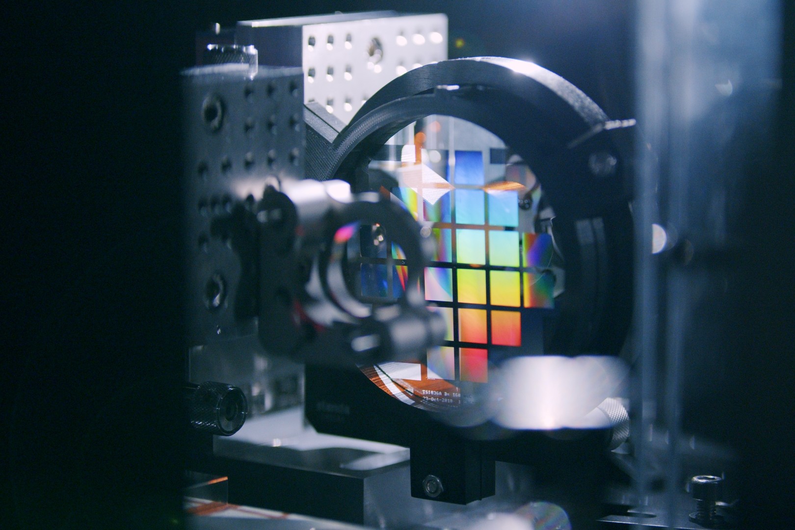
Modern laser technology provides high-power beams at high beam quality which can be utilized for efficient and accurate material processing. In our LENA optics lab an industrial-grade pulsed solid state laser is available. It provides pulse widths between 300 fs and 10 ps at a repetition rate of 200 kHz and a fundamental wavelength of 1040 nm. The ultra-short pulses limit the energy transfer to the crystal lattice during laser processing. That means that the heat-affected zone turns out to be small in comparison to the nanosecond and cw regime. By frequency conversion, shorter wavelengths of 520 and 348 nm can also be generated for different material processing steps.

The laser beam can be focussed onto the sample surface by different objectives. Scanning along the surface can either be realized by a galvanometer scanner, which rapidly deflects the beam by tiltable mirrors, or by moving the sample on a xy-positioner. Equipped with a powerful software, fully automated recipe sequences can be run.

Currently, two main research aspects are explored. On the one hand, the system is used for a LLO process of GaN-based LEDs from sapphire. Sapphire has been established as a reliable and cheap substrate for epitaxial growth of functional GaN layers. However, for certain applications as high-power or structured LEDs, other substrates, e.g., metals or non-transparent semiconductors, are more favourable. By directing strong laser pulses to the backside of the sapphire, the LED film can be separated from the carrier by local evaporation of an intermediate layer between device and substrate. We have recently demonstrated that this process, which is usually conducted with nanosecond pulsed excimer lasers, can be realized with ultrashort pulses at 520 nm.

On the other hand, the system is used for direct structuring of sapphire substrates. µLEDs produced at the Institute are commonly designed as bottom-emitters, i. e. the main direction of light emission is through the underlying sapphire substrate. For efficient use, e. g. coupling into a fibre, it may be beneficial to reduce the sapphire thickness. For this purpose laser-based pre-structuring of the sapphire wafers with high precision from the backside is applied before the epitaxial GaN growth of the device layers. Moreover, the setup can be used for chip separation as the last step in the production chain.

Contact: Jana Hartmann


Foto vom Laser Lift Off Setup, Foto von geliftetem GaN und Foto von mit Laser bearbeitetem Saphir Wafer
Deep Etching

Three-dimensional (3D) architectures like nano/microwires or fins can provide several advantages compared to planar structures: They have a large surface-to-volume ratio, non-polar sidewalls and potentially small footprints which could lead to crystal lattice relaxation. In the Institute 3D architectures are used for optoelectronic (e.g. flexible LEDs), electronic (Field Effect Transistors, FETs) and sensing applications. The structures are produced either by bottom-up (epitaxial growth, see selective area growth in “Epitaxy”) or top-down (i.e. etching) methods. The latter is described in the schematic below. By lithography a chromium layer is structured and used as a hard mask for the ICP-RIE. After the plasma process, the surfaces are very rough making a second step inevitable, which is wet etching in a KOH based solution. This smoothens the surfaces and leads to vertical sidewalls. By this deep etching method, the shape and size of the 3D architectures can be freely selected. Another advantage of the top-down approach is that vertical profiles along the height of the architectures (e.g. axial pn-junctions) are easily feasible: The layer stacks with different material compositions or doping concentrations can be designed based on the desired application and are subsequently grown as planar layers in MOVPE. Due to the planar growth there are no additional limitations (e.g. concerning the material composition) which would definitely emerge during selective 3D growth. After the planar epitaxy the structuring into the favoured shape is realized by deep etching.

Contact:  Jana Hartmann

Schematische Darstellung der Schritte im Ätzprozess zum Tiefätzen von 3D Strukturen
µLED arrays

Gallium Nitride-based (GaN) LEDs have established themselves over the last three decades as the dominant light source for the automotive sector up to general lighting. LED chips have become increasingly efficient and at the same time larger and larger. Today, internal quantum efficiencies of over 90%, close to the theoretical limit, are achieved. Nowadays 300 lumen/watt of white light can be emitted from these LEDs. GaN LEDs will therefore completely substitute all other light sources in the near future.

In contrast to large-area high-performance LEDs, microLEDs (µLEDs) with dimensions of 1 to 50 µm are becoming increasingly interesting, mainly driven by developments in display technology. Beyond this application purpose, many other applications can be derived.

At the Institute of Semiconductor Technology these µLED arrays are developed, fabricated and characterized. The LED arrays are basically chips containing a large number of µLEDs in specific arrangements and including their contact structures. Such a µLED array with 5 µm pixel size is shown in the figure (left). The corresponding chips are connected to in-house developed electronics to create complete integrated systems, such a PCB is shown in the figure (right). The µLED arrays are then controlled via a graphical user interface to create arbitrary light patterns and animations.

The fields of application for this µLED platform at the Institute of Semiconductor Technology are chip-based superresolution microscopy (Chipscope), resolution enhancement of holographic microscopy, optical manipulation of single atoms (EXC QF) and energy-efficient gas and fiber sensors.

Contact: Jan Gülink

Foto von microLED Array und von Platine für array
GaN Electronics

Electrical energy represents a fundamental part of our society today and it is impossible to imagine our everyday life without it. Especially in the course of the conversion to renewable energies, the development of powerful and efficient electrical converters plays an important role. Here, wide-bandgap semiconductor materials such as gallium nitride (GaN) or silicon carbide (SiC) are a key factor for achieving high breakdown voltages and conversion efficiencies.

The excellent material properties of GaN, which is mainly known from its broad application in LEDs, led to the first commercialization of GaN transistors about ten years ago. The concept of these so-called High Electron Mobility Transistors (HEMTs) is based on the superior conductivity of a two-dimensional electron gas, which is automatically formed at the interface between GaN and AlGaN due to internal polarization fields, resulting in excellent transport properties and extremely fast switching times. However, the planar shape of HEMTs and the native normally-on character of the electron gas imposes certain limitations for applications in power electronics, especially in the high voltage range.

At the Institute of Semiconductor Technology, we investigate a novel vertical transistor concept based on regularly arranged GaN nano- and microstructures, which combines numerous potential advantages. The GaN structures are fabricated by deep etching of planar GaN wafers which were grown via metalorganic vapor phase epitaxy (MOVPE). The GaN structures are uniformly coated with a dielectric oxide layer and a wrap-around gate electrode. When a positive voltage is applied to the gate, it opens up a vertical channel close to the surface of the sidewalls by field effect and thus controls the current flow between the top and bottom of the structures. The three-dimensionality of the structures results in an excellent electrostatic control of the channel through the gate. Furthermore, GaN nanostructures allow partial strain relaxation and offer large non-polar surfaces on their sidewalls, which are suitable for the realization of normally-off transistors preferred for safe power switching. At the same time, the vertical architecture is advantageous for high breakdown voltages on a reduced chip area and allows arbitrary scaling of the current flow by parallel integration of many nanostructures in one device.

Several vertical transistors based on GaN nanowires as well as on mechanically more robust GaN fin structures were realized and demonstrate the functionality of the concept. The project is supported by device simulations by the Computational Electronics and Photonics (CEP) group from Bernd Witzigmann at Kassel University.  

Contact: Jana Hartmann

Schematik der Fin FETs, Kontaktiertes Fin FET array, SEM Abbildung des Querschnitts eines Fin FETs

Contact

Are you a representative of the press or politics and have questions about our research? Our scientists will be happy to share their knowledge and expertise with you.


Prof. Dr. Andreas Waag
Speaker of NTC

Phone: +49 531 391 3774
a.waag(at)tu-braunschweig.de

Prof. Dr. Andreas Waag
Photo credits on this page

For All Visitors

Vacancies of TU Braunschweig
Career Service' Job Exchange 
Merchandising

For Students

Term Dates
Courses
Degree Programmes
Information for Freshman
TUCard

Internal Tools

Glossary (GER-EN)
Change your Personal Data

Contact

Technische Universität Braunschweig
Universitätsplatz 2
38106 Braunschweig

P. O. Box: 38092 Braunschweig
GERMANY

Phone: +49 (0) 531 391-0

Getting here

© Technische Universität Braunschweig
Legal Notice Privacy Accessibility

TU Braunschweig uses the software Matomo for anonymised web analysis. The data serve to optimise the web offer.
You can find more information in our data protection declaration.