Technische Universität Braunschweig
  • Study & Teaching
    • Beginning your Studies
      • Prospective Students
      • Degree Programmes
      • Application
      • Fit4TU
      • Why Braunschweig?
    • During your Studies
      • Fresher's Hub
      • Term Dates
      • Courses
      • Practical Information
      • Beratungsnavi
      • Additional Qualifications
      • Financing and Costs
      • Special Circumstances
      • Health and Well-being
      • Campus life
    • At the End of your Studies
      • Discontinuation and Credentials Certification
      • After graduation
      • Alumni
    • For Teaching Staff
      • Strategy, Offers and Information
      • Learning Management System Stud.IP
    • Contact
      • Study Service Centre
      • Academic Advice Service
      • Student Office
      • Career Service
  • Research
    • Research Profile
      • Core Research Areas
      • Clusters of Excellence at TU Braunschweig
      • Research Projects
      • Research Centres
      • Professors‘ Research Profiles
    • Early Career Researchers
      • Support in the early stages of an academic career
      • PhD-Students
      • Postdocs
      • Junior research group leaders
      • Junior Professorship and Tenure-Track
      • Habilitation
      • Service Offers for Scientists
    • Research Data & Transparency
      • Transparency in Research
      • Research Data
      • Open Access Strategy
      • Digital Research Announcement
    • Research Funding
      • Research Funding Network
      • Research funding
    • Contact
      • Research Services
      • Academy for Graduates
  • International
    • International Students
      • Why Braunschweig?
      • Degree seeking students
      • Exchange Studies
      • TU Braunschweig Summer School
      • Refugees
      • International Student Support
      • International Career Service
    • Going Abroad
      • Studying abroad
      • Internships abroad
      • Teaching and research abroad
      • Working abroad
    • International Researchers
      • Welcome Support for International Researchers
      • Service for Host Institutes
    • Language and intercultural competence training
      • Learning German
      • Learning Foreign Languages
      • Intercultural Communication
    • International Profile
      • Internationalisation
      • International Cooperations
      • Strategic partnerships
      • International networks
    • International House
      • About us
      • Contact & Office Hours
      • News and Events
      • International Days
      • 5th Student Conference: Internationalisation of Higher Education
      • Newsletter, Podcast & Videos
      • Job Advertisements
  • TU Braunschweig
    • Our Profile
      • Aims & Values
      • Regulations and Guidelines
      • Alliances & Partners
      • The University Development Initiative 2030
      • Facts & Figures
      • Our History
    • Career
      • Working at TU Braunschweig
      • Vacancies
    • Economy & Business
      • Entrepreneurship
      • Friends & Supporters
    • General Public
      • Check-in for Students
      • CampusXperience
      • The Student House
      • Access to the University Library
    • Media Services
      • Communications and Press Service
      • Services for media
      • Film and photo permits
      • Advices for scientists
      • Topics and stories
    • Contact
      • General Contact
      • Getting here
  • Organisation
    • Presidency & Administration
      • Executive Board
      • Designated Offices
      • Administration
      • Committees
    • Faculties
      • Carl-Friedrich-Gauß-Fakultät
      • Faculty of Life Sciences
      • Faculty of Architecture, Civil Engineering and Environmental Sciences
      • Faculty of Mechanical Engineering
      • Faculty of Electrical Engineering, Information Technology, Physics
      • Faculty of Humanities and Education
    • Institutes
      • Institutes from A to Z
    • Facilities
      • University Library
      • Gauß-IT-Zentrum
      • Professional and Personnel Development
      • International House
      • The Project House of the TU Braunschweig
      • Transfer Service
      • University Sports Center
      • Facilities from A to Z
    • Equal Opportunity Office
      • Equal Opportunity Office
      • Family
      • Diversity for Students
  • Search
  • Quicklinks
    • People Search
    • Webmail
    • cloud.TU Braunschweig
    • Messenger
    • Cafeteria
    • Courses
    • Stud.IP
    • Library Catalogue
    • IT Services
    • Information Portal (employees)
    • Link Collection
    • DE
    • EN
    • Instagram
    • YouTube
    • LinkedIn
    • Mastodon
    • Bluesky
Menu
  • Organisation
  • Faculties
  • Faculty of Electrical Engineering, Information Technology, Physics
  • Institutes
  • Institute of Semiconductor Technology
  • Institute
  • The Team
  • Professors
Logo Institut für Halbleitertechnik der TU Braunschweig
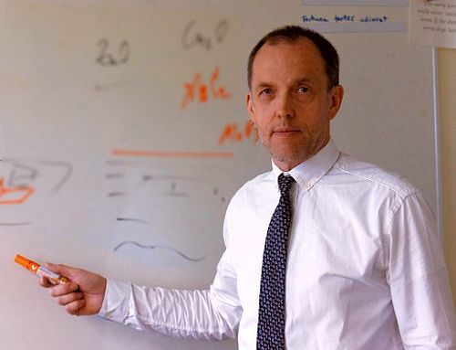
Prof. Dr. Andrey Bakin
  • Professors
    • Prof. Dr. Andreas Waag
    • Prof. Dr. rer. nat. Tobias Voss
    • Prof. Dr. rer. nat. Stefanie Kroker
    • Prof. Dr. Andrey Bakin
    • Prof. Dr. Erwin Peiner
    • Prof. Dr. J. Daniel Prades

Prof. Dr. Andrey Bakin

Andrey Bakin

TU Braunschweig, Institut für Halbleitertechnik
Hans-Sommer-Straße 66
38106 Braunschweig 


A.Bakin@tu-braunschweig.de

Research:

  • 2D-Materials and their Stacks (in Cooperation with PTB Braunschweig) Gallenene, Graphen, new 2D Materials and Technologies ...
  • Thin Film Technology (VPE, PE-ALD, MOCVD, PVT, chem. growth, MBE)
  • Functional Oxides (Cu2O, ZnO, Ga2O3, MoO3, Al2O3, SiO2)
  • Nanostructures, layers and crystals for Optoelectronics, Nanometrology, Sensoric, Photovoltaic:  II/VI, III/N, SiC, III/V ...
  • Sustainable Energy Conversion using Earth-Abundant Materials
  • Plasma Profiling Time-of-Flight Mass Spectrometry (ppTOF-MS) (Research Center  LENA)

 Publications:

Researcher Profile at Google Scholar 

Web of Science ResearcherID


Teaching:

  • Thin Film Technology: Lectures and practical course
  • Semiconductor Technology: Lectures and practical courses
  • Nano- und Polycrystalline Materials: Lectures and practical course
  • Nanotechnology in Microelectronics: Lectures and practical course
  • Electronic Technology I and II: Lab (jointly with Prof. Dr. Waag)
  • NanoSystemsEngineering: Lab and Colloquium
  • NanoSystemsEngineering: Seminar for Bachelor/Master 
  • Semiconductor Technology: Studienseminar
  • Master-/Bachelor-works (can be started immediately):

                        2D Materials (in cooperation with PTB Braunschweig)

CV:

Andrey Bakin, received the Diploma of Engineer and Ph.D. degrees, both from the St.-Petersburg Electrotechnical University (ETU "LETI"), Russia in 1981 and 1985, respectively, working there till 1988 on growth of IV/VI-compound semiconductors (Pb-Sn-Te) and IR-sensors fabrication. One year in 1988-1989 and three months in 1993 he worked at the Institut für Halbleitertechnik (Institute for Semiconductor Technology) of the Technische Universität Braunschweig, Germany, where his main field of interest was epitaxial growth of III/V-compound semiconductors. From 1989 to 1994 he worked as senior researcher and Assistant Professor at the St.-Petersburg Electrotechnical University, where he worked on the development sublimation growth of SiC crystals. In 1994-1995 he worked at the Department of Physics and Measurement Technology of Linköping University, Sweden on the investigation of silicon carbide HTCVD, CVD and sublimation growth. From 1995 to 1998 he was an Associate Professor at the St.-Petersburg Electrotechnical University, where he managed and worked on the advancement of SiC sublimation growth and cutting edge technological equipment design and development. In 1998 he joined Institut für Halbleitertechnik (Institute for Semiconductor Technology) of the Technische Universität Braunschweig, Germany, where his main field of interest is epitaxy of compound semiconductors ( II/VI-, III/V-, III/N- and IV/IV) using VPE, MBE, MOVPE, PEALD as well as chemical approaches for micro- and optoelectronics, sensoric, sustainable energy conversion. At the Technical University of Braunschweig he completed his Habilitation (post doctoral thesis).

  • Habilitation (PostDoctoral Thesis): "Gas phase growth of compound semiconductors"

Publications:

  • S. Metzner, B. Kästner, M. Marschall, G. Wübbeler, S. Wundrack, A. Bakin, A. Hoehl, E. Rühl and C. Elster. Assessment of sub-sampling schemes for compressive nano-FTIR imaging . 2022, IEEE Transactions on Instrumentation and Measurement , Vol. 71, DOI: 10.1109/TIM.2022.3204072
  • S. Metzner, B. Kästner, M. Marschall, G. Wübbeler, S. Wundrack, A. Bakin, A. Hoehl, E. Rühl and C. Elster. Assessment of sub-sampling schemes for compressive nano-FTIR imaging . 2022, arXiv preprint arXiv:2204.05531, https://arxiv.org/pdf/2204.05531.pdf
  • T. Bordignon, M. Fregolent, C. De Santi, K. Strempel, A. Bakin, A. Waag, G. Meneghesso, E. Zanoni, M. Meneghini. Dynamic and Capacitive Characterization of 3D GaN n-p-n Vertical Fin-FETs. 2021, ieeexplore.ieee.org, DOI: 10.1109/WiPDA49284.2021.9645108
  • S. Wundrack, D. M. Pakdehi, W. Dempwolf, N. Schmidt, K. Pierz, L. Michaliszyn, H. Spende, A. Schmidt, H. W. Schumacher, R. Stosch, A. Bakin. Liquid metal intercalation of epitaxial graphene: large-area gallenene layer fabrication through gallium self-propagation at ambient conditions . 2021, APS Physical Review Materials,  https://journals.aps.org/prmaterials/abstract/10.1103/PhysRevMaterials.5.024006
  • H. Spende, C. Margenfeld, T. Meyer, I.M. Clavero, H. Bremers, A. Hangleiter, M. Seibt, A. Waag, A. Bakin. Plasma Profiling Time-of-Flight Mass Spectrometry for Fast Elemental Analysis of Semiconductor Structures with Depth Resolution in the Nanometer Range. 2020, Semiconductor Science and Technology  https://doi.org/10.1088/1361-6641/ab6ac0
  • S. Wundrack, D. M. Pakdehi, W. Dempwolf, N. Schmidt, K. Pierz, L. Michaliszyn, H. Spende, A. Schmidt, H. W. Schumacher, R. Stosch, A. Bakin. Liquid metal intercalation of epitaxial graphene: large-area gallenene layer fabrication through gallium self-propagation at ambient conditions . 2019, https://arxiv.org/abs/1905.12438
  • Q. H. Nguyen, C. Mandla, W. Emer, F. Yu, A. Bakin and M. Tornow .

    Organophosphonate Functionalization of Al2O3-Coated Nanopores. 2019, DOI: 10.1109/NEMS.2019.8915589

  • M. F. Fatahilah, F. Yu, K. Strempel, F. Römer, D. Maradan, M. Meneghini, A. Bakin, F. Hohls, H. W. Schumacher, B. Witzigmann, A. Waag, H. S. Wasisto. Top-down GaN nanowire transistors with nearly zero gate hysteresis for parallel vertical electronics. 2019, Nature Scientific Reports
     
  • D. M. Pakdehi, K. Pierz, S. Wundrack, J. Aprojanz, T. T. N. Nguyen, T. Dziomba, F. Hohls, A. Bakin, R. Stosch,C. Tegenkamp, F. J. Ahlers,  H. W. Schumacher. Homogeneous Large-Area Quasi-freestanding Monolayer and Bilayer Graphene on SiC. 2019, ACS Appl. Nano Mater.  DOI: 10.1021/acsanm.8b02093
  • S. Wundrack, D. M. Pakdehi, P. Schädlich, F. Speck, K. Pierz, T. Seyller, H. W. Schumacher, A. Bakin, R. Stosch. Probing the structural transition from buffer-layer to quasifreestanding monolayer graphene by raman spectroscopy. Physical Review B, 99, 045443, 2019 
  • D. M. Pakdehi, K. Pierz, S. Wundrack, J. Aprojanz, T. T. N. Nguyen, T. Dziomba, F. Hohls, A. Bakin, R. Stosch,C. Tegenkamp, F. J. Ahlers,  H. W. Schumacher. Homogeneous Large-Area Quasi-freestanding Monolayer and Bilayer Graphene on SiC. 2018, arXiv.org, arxiv.org/abs/1811.04998 [cond-mat.mtrl-sci]
  • M. Kruskopf, K. Pierz, D. M. Pakdehi, S. Wundrack, R. Stosch, A. Bakin, H. W. Schumacher. A morphology study on the epitaxial growth of graphene and its buffer layer. Thin Solid Films, V. 659, 2018, pp. 7-15, doi: 10.1016/j.tsf.2018.05.025
  • F. Yu, K. Strempel, M. F. Fatahilah, H. Zhou, F. Römer, A. Bakin, B. Witzigmann, H. W. Schumacher, H.S. Wasisto, A. Waag. Normally Off Vertical 3-D GaN Nanowire MOSFETs With Inverted p-GaN Channel. IEEE Transactions on Electron Devices, 2018,  doi: 10.1109/TED.2018.2824985
  • J Xu, M Bertke, A Gad, F Yu, G Hamdana, A Bakin, E Peiner .Fabrication of ZnO Nanorods on MEMS Piezoresistive Silicon Microcantilevers for Environmental Monitoring. Multidisciplinary Digital Publishing Institute Proceedings 1 (4), 290, 2017
  • B. Liu, H. Yan, R. Stosch, B. Wolfram, M. Bröring, A. Bakin, M. Schilling, P. Lemmens. Modelling plexitons of periodic gold nanorod arrays with molecular components.  Nanotechnology, 2017, doi: 10.1088/1361-6528/aa67d8M.
     
  • M. Kruskopf, K. Pierz, D. M. Pakdehi, S. Wundrack, R. Stosch, A. Bakin, H. W. Schumacher. Tailoring the SiC surface - a morphology study on the epitaxial growth of graphene and its buffer layer . 2017, arXiv.org, arxiv.org/abs/1704.08078 [cond-mat.mtrl-sci]
  • F. Yu, S. Yao, F. Römer, B. Witzigmann, T. Schimpke, M. Strassburg, A. Bakin, H. W. Schumacher, E. Peiner, H.S. Wasisto, A. Waag. GaN nanowire arrays with nonpolar sidewalls for vertically integrated field-effect transistors.  Nanotechnology, 2017, doi: 10.1088/1361-6528/aa57b6
  • F Yu, D Rümmler, J Hartmann, L Caccamo, T Schimpke, M Strassburg, AE Gad, A Bakin, H-H Wehmann, B Witzigmann, HS Wasisto, A Waag. Vertical architecture for enhancement mode power transistors based on GaN nanowires.  Applied Physics Letters, 2016, V. 108, issue 21, 213503-1 - 5, doi: 10.1063/1.4952715
  • M. Abdelfatah, J. Ledig, A. El-Shaer, A. Sharafeev, P. Lemmens, M. M. Mosaad, A. Waag, and A. Bakin. Effect of Potentiostatic and Galvanostatic electrodeposition modes on the basic parameters of solar cells based on Cu2O thin films.  Electrochemical Society Journal of Solid State Science and Technology, 2016, V. 5, issue 6, Q183-Q187, doi: 10.1149/2.0191606jss
  • M. Abdelfatah, J. Ledig, A. El-Shaer, A. Wagner, V. M. Borras, A. Sharafeev, P. Lemmens, M. M. Mosaad, A. Waag, and A. Bakin. Fabrication and Characterization of low cost Cu2O/ZnO solar cells for sustainable photovoltaics with earth abundant materials. Solar Energy Materials and Solar Cells, Elsevier, SOLMAT8042, 2016, V. 145, pp. 454-461; doi: 10.1016/j.solmat.2015.11.015
  • M. Abdelfatah, J. Ledig, A. El-Shaer, A. Wagner, A. Sharafeev, P. Lemmens, M. M. Mosaad, A. Waag, and A. Bakin. Fabrication and Characterization of flexible solar cell from electrodeposited Cu2O thin films on plastic substrate. Solar Energy, Elsevier, 122 (2015); DOI: dx.doi.org/10.1016/j.solener.2015.11.002
  • H.S. Wasisto, F. Yu, L. Doering, S. Völlmeke, U. Brand, A. Bakin, A. Waag, E. Peiner. Fabrication of wear-resistant silicon microprobe tips for high-speed surface roughness scanning devices. SPIE Microtechnologies, 951723-951723-7, (2015)
  • A. Wagner, M. Stahl, N. Erhardt, A. Fahl, J. Ledig, A. Waag, and A. Bakin. Oxides for sustainable photovoltaics with earth-abundant materials. Invited Paper. Proc. SPIE 8987, Oxide-based materials and Devices V, 989726 (2014); doi: 10.1117/12.2044734
  • A. Bakin, A. Behrends, A. Wagner, A. Waag. Fabrication of ZnO Nanostructures. Invited Chapter in “Zinc Oxide Nanostructures“ ed. by M. Willander, Pan Stanford Publishing Pte Ltd, ISBN 978-981-4411-33-2 (2014) 
  • M. Lafrentz, D. Brunne, V. V. Pavlov, A. V. Rodina, R. V. Pisarev, D. R. Yakovlev, A. Bakin, and M. Bayer. Second harmonic generation spectroscopy of excitons in ZnO. Phys. Rev. B 88, 235207 (2013)
  • A. Wagner, H. Scherg-Kurmes, A. Waag and A. Bakin. Vapour phase epitaxy of Cu2O on a-plane Al2O3. Physica Status Solidi, Volume 2, Issue 12 (2013) 
  • M. Lafrentz, D. Brunne, B. Kaminski, V. V. Pavlov, A. V. Rodina,R. V. Pisarev, D. R. Yakovlev, A. Bakin, and M. Bayer. Magneto-Stark effect of excitons as origin of second harmonic generation in ZnO. Physical Review Letters (PRL), 110, 116402 (2013)
  • M. S. Mohajerani, M.A. Reschikov, A. Behrends, A. Bakin, S. Kück, A. Waag. Determination of zinc concentration in GaN:Zn,Si from
    photoluminescence.
    Phys. Status Solidi C 10, No. 3, 523–526 (2013)
  • H. Horn, A. Balocchi,X. Marie, A. Bakin, A. Waag, M. Oestreich, J. Hübner. Spin noise spectroscopy of donor-bound electrons in ZnO. Physical Review B, 87, No. 4, 054312 (2013)
  • M.A. Reschikov, J. D. McNamara, A. Behrends, M. S. Mohajerani, A. Bakin, A. Waag. Higher than 90% internal quantum efficiency of photoluminescence in GaN:Si,Zn. Phys. Status Solidi C 10, No. 3, 507–510 (2013)
  • M.A. Reschikov, M. Foussekis, J. D. McNamara, A. Behrends, A. Bakin, A. Waag. Determination of the absolute internal quantum efficiency of photoluminescence in GaN co-doped  with Si and Zn. Applied Physics, 111, iss. 7 (2012) jap.aip.org/resource/1/japiau/v111/i7/p073106_s1
  • A. Behrends, A. Wagner, M. A. M. Al-Suleiman, H.-J. Lugauer, M. Strassburg, R. Walter, A. Weimar, Andreas Waag, and A. Bakin. Transparent conductive Ga-doped ZnO films fabricated by MOCVD.  Phys. Status Solidi A, (2012) DOI 10.1002/pssa.201127324
  • A. Wagner, A. Behrends, A. Waag, A. Bakin.  Two step deposition method with a high growth rate for ZnO nanowire arrays and its application in photovoltaics. Thin Solid Films, 520 (14) , pp. 4637-4641 (2012)
  • A. Wagner, A. Bakin, T. Otto, M. Zimmermann, B. Jahn,  A. Waag.   Fabrication and Characterization of Nanoporous ZnO Layers for Sensing Applications. Thin Solid Films, 520 (14) , pp. 4662-4665 (2012)
  • A. Behrends,  J. Ledig, M. A. M. Al-Suleiman, S. Peters, A. M. Racu, W. Schmunk, H. Hofer, S. Kück, A. Bakin, A. Waag. Zn doped GaN for single-photon emission.  Phys. Status Solidi C, (2012)  9 (3-4) , pp. 1024-1027
  • A. Bakin, A. Waag.   ZnO Epitaxial Growth. Invited Chapter for “Comprehensive Semiconductor Science and Technology“ Encyclopaedia ELSEVIER, edited by R. Fornari (2011)  ISBN: 978-0-444-53143-8
  • M.A. Reschikov, A.G. Willuard, A. Behrends, A. Bakin, A. Waag.   Extremely high absolute internal quantum efficiency of photoluminescence in co-doped GaN:Zn,Si. Applied Physics Letters, 99, 171110 (2011)
  • N. Heuck, A. Langer, A. Stranz, G. Palm, R. Sittig, A. Bakin, and A. Waag. Analysis and Modeling of Thermomechanically Improved Silver-Sintered Die-Attach Layers Modified by Additives. IEEE TRANSACTIONS ON COMPONENTS, PACKAGING AND MANUFACTURING TECHNOLOGY, (2011), 1 (11) , art. no. 6045323 , pp. 1846-185
  • V. Petukhov, A. Bakin, J. Tsiaosusis, J. Rothman, S. Ivanov, J. Stoemenos, A. Waag.   Implementation of ZnO/ZnMgO strained-layer superlattice for ZnO heteroepitaxial growth on sapphire. Jornal of Crystal Growth (2011) 323 (1) , pp. 111-113V. 
  • M.A.Bobrov, A.A.Toropov, S.V.Ivanov, A. ElShaer, A. Bakin, A. Waag.   Excitonic Spectrum of the ZnO/ZnMgO Quantum Wells. Semiconductors (2011) Vol. 45, No. 6, pp. 766–770
  • V. Petukhov, J. Stoemenos, J. Rothman, A. Bakin, A. Waag.   Interpretation of transport measurements in ZnO-thin films. Appl. Phys. A., V. 102, n. 1 (2011) pp. 161-168
  • V. Petukhov, J. Stoemenos, J. Rothman, A. Bakin, A. Waag.   Erratum: Interpretation of transport measurements in ZnO-thin films. Appl. Phys. A., V. 102, n. 1 (2011) pp. 251
  • A. Bakin, A. Behrends, A. Waag, H.-J. Lugauer, A. Laubusch and K. Streubel.   ZnO-GaN Hybrid Heterostructures as Potential Cost Efficient LED Technology. IEEE (Invited Paper for a special volume), Proceedings of the IEEE, 2010, vol. 98, N. 7, pp. 1281-1287.s
  • A. Behrends, A. Bakin, A. Waag, H.-S. Kwack, and Le Si Dang.   Electroluminescence from n–ZnO/p–GaN Hybrid LED. Phys. Stat. Sol. C V. 7, Iss. 6  (2010) 1709-1711
  • N. Heuck, G. Palm, T. Sauerberg, A. Waag, A. Bakin   SiC-Die-Attachment for High Temperature Applications. Materials Science Vols. 645-648, Trans Tech Publications, 2010, pp. 741-744.
  • S. Fündling, Ü. Sökmen, A. Behrends, M. Al-Suleiman, S. Merzsch, S.F. Li, A. Bakin, H.-H. Wehmann, A. Waag, J. Lähnemann, U. Jahn, A. Trampert, H. Riechert   GaN and ZnO nanostructures. Phys. Stat. Sol. B 247 (2010) 2315-2328
  • M. A. M. Al-Suleiman, A. Bakin, A. Waag   Mechanisms for high internal quantum efficiency of ZnO nanorods. Journal of Applied Physics, 106 (2009) 063111
  • Robin, I.C., Marotel, P., El-Shaer, A.H., Petukhov, V., Bakin, A., Waag, A., Lafossas, M., Garcia, J., Rosina, M., Ribeaud, A., Brochen, S., Ferret, P., Feuillet, G.   Compared optical properties of ZnO heteroepitaxial, homoepitaxial 2D layers and nanowires. Journal of Crystal Growth, V. 311, (2009), iss. 7, pp. 2172-2175
  • A.Behrends, A. Bakin, A.Waag.   Investigation of ZnO Nanopillars Fabrication in a new Thomas Swan Close Coupled Showerhead MOCVD Reactor. Microelectronics Journal, 40 (2009) 280-282
  • M Willander,O Nur,Q X Zhao,L L Yang, M Lorenz, B Q Cao,JZuiga Perez, C Czekalla, G Zimmermann,M Grundmann,A Bakin, A Behrends, M Al-Suleiman, A El-Shaer, A Che Mofor, B Postels, A Waag,N Boukos,A Travlos,H S Kwack, ,J Guinard and D Le Si Dang     Topical Review: Zinc oxide nanorod based photonic devices: recent progress in growth,light emitting diodes and lasers. Nanotechnology, 20 (2009) 332001 (40pp)
  • A. Bakin, A. Wagner, E. Schlenker, B. Postels, M. Al-Suleiman, A. Behrends, A.-H. Elshaer, V. Petukhov, A.Waag.   ZnO Nanostructures and Thin Layers for Device Applications. ECS Transactions, Volume 16(12) The Electrochemical Society (2008) 107
  • Fündling, S., Soekmen, U., Peiner, E., Weimann, T., Hinze, P., Jahn, U., Trampert, A., Riechert, H., Bakin, A., Wehmann, H.-H., Waag, A.     Gallium nitride heterostructures on 3D structured silicon. Nanotechnology, 19 (40) (2008) 405301
  • Hofstetter, D., Thron, R., El-Shaer, A.-H., Bakin, A., Waag, A.  Demonstration of a ZnO/MgZnO- based one-dimensional photonic crystal multlquantum well laser. Applied Physics Letters, 93 (10), (2008)101109
  • Fündling, S., Sökmen, U., Peiner, E., Weimann, T., Hinze, P., Jahn, U., Trampert, A., Riechert, H., Bakin, A., Wehmann, H.-H., Waag, A.   Demonstration of a ZnO/MgZnO-based one-dimensional photonic crystal multiquantum well laser. Applied Physics Letters, 93 (10), (2008) 101109
  • E. Schlenker,A. Bakin,T. Weimann, P.Hinze, D.H.Weber,A. Gölzhäuser,H-H. Wehmann and A. Waag   On the difficulties in characterizing ZnO nanowires, Nanotechnology 19 (2008) 365707
  • Eva Schlenker,Andrey Bakin, Hergo-Heinrich Wehmann, Augustine Che Mofor, Arne Behrends, Andreas Waag, Thomas Weimann, Peter Hinze, Alexander Melnikov and Andreas D. Wieck   Electrical Properties of ZnO-Based Nanostructures, Journal of the Korean Physical Society, Vol. 53, No. 1, July 2008, pp. 119-122
  • E. Schlenker, A. Bakin, H.-H. Wehmann, M. Al-Suleiman, and A. Waag  Investigation of Mn doped ZnO Nanopowder, Appl. Phys. A, 2008, V. 91, Iss. 4, pp. 375-378
  • B. Postels, A. Kasprzak, T. Buergel, A. Bakin, E. Schlenker, H.-H. Wehmann, A. Waag   Dye-sensitized solar cells on the basis of ZnO nanorods. Journal of the Korean Physical Society Vol. 53, No. 1, (2008) 115-118
  • B. Postels, H-H Wehmann, A. Bakin, T. Weimann, P.Hinze, A. Waag  Electrodeposition of ZnO nanorods for device application, Appl. Phys. A, 2008, V. 91, Iss. 4, pp. 595-599
  • Robin, I.C., Tavares, C., Rothman, J., Feuillet, G., El-Shaer, A.H., Bakin, A., Waag, A., Dang, L.S.   Structural and spectroscopic properties of a 2 inch ZnO-on-sapphire epiwafer grown by using molecular beam epitaxy. Journal of the Korean Physical Society, 53 (5 PART 2) (2008), pp. 2877-2879
  • C. Bekeny, T. Voss, B. Hilker, J. Gutowski, R. Hauschild, H. Kalt, B. Postels, A. Bakin, A. Waag.   Microscopic origin oft he near-band-edge emission in aqueos chemically-grown ZnO nanorods. Journal of the Korean Physical Society 53(5), (2008) 2867-2869
  • Ivanov, S.V., El-Shaer, A., Al-Suleiman, M., Bakin, A., Waag, A., Lyublinskaya, O.G., Shmidt, N.M., Listoshin, S.B., Kyutt, R.N., Ratnikov, V.V., Terentyev, A.Ya., Ber, B.Ya., Komissarova, T.A., Ryabova,L.I., Khokhlov, D.R.   Studies of N-doped p-ZnO layers grown on c-sapphire by radical source molecular beam epitaxy. Journal of the Korean Physical Society, 53 (5 PART 2), (2008) 3016-3020.
  • A. Bakin, J. Kioseoglou , B. Pecz, A. El-Shaer, A.-C. Mofor, J. Stoemenos, A. Waag  Misfit reduction by a Spinel layer formed during the epitaxial growth of ZnO on Sapphire using a MgO buffer layer, J. Crystal Growth, 308, 2007, pp. 314–320
  • A.Bakin, A. El-Shaer, A.C.Mofor, M. Al-Suleiman, E. Schlenker, and A.Waag ZnMgO-ZnO Quantum Wells Embedded in ZnO Nanopillars: Towards Realisation of Nano-LEDs , Phys. Stat. Solidi (c), vol. 4, n1, 2007, pp. 158-161
  • T.V. Shubina, A.A. Toropov, O.G. Lublinskaya, S.B. Listoshin, A.A. Sitnikova, El-Shaer, M. Al-Suleiman, A. A. Bakin, A. Waag, E.V. Lutsenko, G.P. Yablonskii, J.P. Bergman, G Pozina, B. Monemar, S.V. Ivanov.   Exciton recombination dynamics and lasing in ZnMgO/ZnO single quantum well structures , Applied Phys. Lett. 91 (2007) 201104 (1-3)
  • D. Hofstetter, Y. Bonetti, F. R. Giorgetta, A-H. El-Shaer, A. Bakin, A. Waag, R. Schmidt-Grund, M. Schubert, and M. Grundmann  Demonstration of an ultraviolet ZnO-based optically pumped 3rd order distributed feedback laser, Appl. Phys. Lett. 91, 2007, 111108
  • V. Petukhov, A. Bakin, A.-H. El-Shaer, A.-C. Mofor, and A. Waag  Etch-Pit Density Investigation on Both Polar Faces of ZnO Substrates, Electrochemical and Solid-State Letters, vol. 10, n. 12 2007
  • D. H. Weber, A. Beyer, B. Völkel, A. Gölzhäuser, E. Schlenker, A. Bakin, A. Waag Determination of the specific resistance of individual freestanding ZnO nanowires with the low energy electron point source microscope APPLIED PHYSICS LETTERS, 2007, 91, 253126
  • M. Al-Suleiman, A. El-Shaer, A. Bakin, H.-H.Wehmann and A.Waag  Properties of V-implanted ZnO nanorods, Appl. Phys. Lett. 91, 2007, 081911
  • B. Piechal, J. Yoo, A-H. Elshaer, A-C. Mofor, G-C. Yi, A. Bakin, A. Waag, F. Donatini, Le Si Dang  Cathodoluminescence of single ZnO nanorod heterostructures, Phys. Stat. sol. (b), V. 244, Iss. 5, 2007, pp. 1458-1461
  • E. Schlenker, A. Bakin, H. Schmid, W. Mader, S. Sievers, M. Albrecht, C. Ronning, S. Müller, M. Al-Suleiman, B. Postels, H. Wehmann, U. Siegner, A. Waag  Properties of V-implanted ZnO nanorods, Nanotechnology, 2007, vol. 18, 125609
  • B. Postels, H-H. Wehmann, A. Bakin, M. Kreye, D. Fuhrmann, J. Blaesing, A. Hangleiter, A. Krost and A. Waag Controlled low temperature fabrication of ZnO nanopillars with a wet-chemical approach, Nanotechnology, *18*, 195602 (2007)
  • Werner Prost, Victor Khorenko, Augustine-Che Mofor , Stefan Neumann, Artur Poloczek, Andreas Matiss, Andrey Bakin, Andreas Schlachetzki, and Franz-Josef Tegude High Performance III/V RTD and PIN Diode on a Silicon (001) substrate, Journal Applied Physics A: Materials Science and Processing, Springer, vol. 87, n. 3, 2007, pp. 539-544
  • A. Bakin , A. Che Mofor, A. El-Shaer, and A. Waag Vapour Phase Transport Growth of ZnO Layers and Nanostructures , J. Superlattices and Microstructures, Elsevier, Volume 42, Issues 1-6, 2007, pp. 33-39
  • A. Bakin ZnO Nanostructures, thin Films and Devices Invited Plenary Talk, E-MRS Fall Meeting, Warsaw, 3-8 Sepember, 2006
  • A. El-Shaer, A. Bakin, M. Al-Suleiman, S. Ivanov , A. Che Mofor, and A. Waag Growth of wide band gap wurtzite ZnMgO epilayers on (0001) Al2O3 by radical-source molecular beam epitaxy , J. Superlattices and Microstructures, Elsevier, Volume 42, Issues 1-6, 2007, pp. 129-133
  • A. C. Mofor, A. S. Bakin, B. Postels, M. Suleiman, A. Elshaer, A. Waag Growth of ZnO Layers for Transparent and Flexible Electronics , J. Superlattices and Microstructures, Elsevier, 2006 (in press)
  • A. El-Shaer, A. Bakin, A. Che Mofor, J. Stoimenos, B. Pécz, and A. Waag Layer by layer growth of ZnO on (0001) sapphire substrates by radical-source molecular beam epitaxy , J. Superlattices and Microstructures, Elsevier, Volume 42, Issues 1-6, 2007, pp. 158-164
  • B. Pecz, A. El-Shaer, A. Bakin, A.-C. Mofor, J. Stoemenos and A. Waag Structural characterization of ZnO films grown by Molecular Beam Epitaxy on Sapphire with MgO buffer , JAP 100, 103506, 2006
  • T. Voss, C. Bekeny, L. Wischmeier, H. Gafsi, S. Börner, W. Schade, A. C. Mofor, A. S. Bakin, A. Waag Influence of exciton-phonon coupling on the energy position of the near bandedge photoluminescence of ZnO nanowires , JAP 2006
  • S.V. Ivanov, A. El-Shaer, T.V. Shubina, S.B. Listoshin, A. Bakin, and A. Waag Growth kinetics and properties of ZnO/ZnMgO heterostruc-tures grown by radical-source molecular beam epitaxy , Phys. Stat. Solidi (c) 4, No. 1, 2007, pp. 154–157
  • E. Schlenker, A. Bakin, B. Postels, A.C. Mofor, M. Kreye, C. Ronning, S. Sievers, M. Albrecht, U. Siegner, R. Kling, A. Waag Magnetic characterisation of ZnO doped with Vanadium , J. Superlattices and Microstructures, Elsevier, Volume 42, Issues 1-6, 2007, pp. 236-241
  • A. C. Mofor, A. Bakin, U. Chejarla, E. Schlenker, A. El-Shaer, G. Wagner, N. Boukos, A. Travlos and A. Waag Fabrication of ZnO Nanorod-based p-n Heterojunction on SiC Substrate , Superlattices and Microstructures, Elsevier, vol. 42, iss. 1-6, 2007, pp. 415-420
  • A. El-Shaer, A. Bakin, E. Schlenker, A. C. Mofor, G. Wagner, S. A. Reshanov and A. Waag Fabrication and characterization of n-ZnO on p-SiC heterojunction diodes on 4H-SiC substrates , J. Superlattices and Microstructures, Elsevier, Volume 42, Issues 1-6, 2007, pp. 387-391
  • B. Postels, M. Kreye, H.-H. Wehmann, A. Bakin, N. Boukos, A. Travlos, D. Fuhrmann, A. Hangleiter, A. Waag Selective growth of ZnO nanorods in aqueous solution , J. Superlattices and Microstructures, Elsevier, 42, 2007, pp. 425-439
  • A C Mofor, A El-Shaer, M Suleiman, A Bakin and A Waag A two-step obtainment of quantum confinement in ZnO nanorods , Nanotechnology, 17, 2006, pp. 4859-4862
  • A. C. Mofor, A. S. Bakin, A. El-Shaer, D. Fuhrmann, F. Bertram, A. Waag Vapour Phase Growth of ZnO Nanorods , Appl. Phys. A, DOI: 10.1007/s00339-007-3961-5 (2007)
  • A. El-Shaer, A. Bakin, A. Che Mofor, J. Bläsing, A. Krost, J. Stoimenos, B. Pecz, M. Kreye, A. Waag H2O2-Molecular Beam Epitaxy of high quality ZnO Journal Applied Physics A: Materials Science and Processing, Springer 88, 2007, 57
  • A.C. Mofor, F. Reuß, A. El-Shaer, R. Kling, E. Schlenker, A. Bakin, H. Ahlers, U. Siegner, S. Sievers, M. Albrecht, W. Schoch, N. Izyumskaya, V. Avrutin, W. Limmer, J. Eisenmenger, Th. Mueller, P. Ziemann, and A. Waag Magnetism in Zn(TM)O layers and nanorods grown on Sapphire , Journal Applied Physics A: Materials Science and Processing, Springer, vol. 88, 2007, pp. 161-166
  • A. Bakin. SiC homoepitaxy and heteroepitaxy , Invited Chapter in the book: "SiC Materials and Devices – vol. 1", ed. by M. S. Shur, S. L. Rumyantsev and M. E. Levinshtein, World Sci. (2006). ISBN 981-256-835-2
  • A. C. Mofor , A. S. Bakin, A. Elshaer, D. Fuhrmann, F. Bertram, A. Hangleiter, J. Christen and A. Waag Catalyst-free Vapor-phase transport growth of vertically aligned ZnO nanorods on 6H-SiC and (11-20) Al2O3 , Phys. Stat. Solidi, (c) 3, No. 4, 2006, pp. 1046–1050.
  • A. El Shaer, A. Bakin, A. Che Mofor, J. Bläsing, A. Krost, J. Stoimenos, B. Pécz, M. Kreye, M. Heuken, and A. Waag CBE Growth of High-Quality ZnO Epitaxial Layers , Phys. Stat. Solidi (b), V. 243, no.4, 2006, pp 768-772 .
  • A.C. Mofor, F. Reuss, A. El-Shaer, H. Ahlers, U. Siegner, A. Bakin, W. Limmer, J. Eisenmenger, Th. Mueller, P. Ziemann, and A. Waag A Study of ZnMnO as a material for magneto- and spin-electronics , Phys. Stat. Solidi (c), V.3, no. 4, 2006, pp. 1104-1108.
  • C. Klingshirn,  H. Priller, M. Decker, J. Brückner, H. Kalt, R. Hauschild, J. Zeller, A. Waag, A. Bakin, H. Wehmann,  K. Thonke, R. Sauer, R. Kling, F. Reuss, Ch. Kirchner. Excitonic Properties of ZnO, Chapter in: Adnvances in Solid State Physics, Volume 45, 2006, pp 275-287
  • A. Che Mofor, A. El-Shaer, A. Bakin, A. Waag, H. Ahlers, U. Siegner, S. Sievers, M. Albrecht, W. Schoch, N. Izyumskaya, V. Avrutin, S. Sorokin, S. Ivanov, J. Stoimenos. Magnetic Property investigations on Mn-doped ZnO layers on sapphire , J. Applied Physics Letters,  87, 2005, 062501.
  • A. Bakin, A. El-Shaer, A. Che Mofor, M. Kreye, A. Waag, F. Bertram, J. Christen, J. Stoimenos. MBE growth of ZnO layers on sapphire employing hydrogen peroxide as an oxidant , J. of Crystal Growth, V. 287, n. 1, 2006, pp. 7-11.
  • A. Che Mofor, A. El-Shaer , A. Bakin, H.-H. Wehmann, A. Waag, H. Ahlers, U. Siegner, S. Sievers, M. Albrecht, W. Schoch, N. Izyumskaya, V. Avrutin, J. Stoimenos. Magnetic Property Investigation of ZnMnO , J. Superlattices and Microstructures, Elsevier, V. 39, Iss. 1-4, 2006, pp. 381-386 .
  • O. Schmidt, A. Geis, P. Kiesel, N. Johnson, A. Bakin, A. Waag, and G. Doehle. Analysis of a conducting channel at the native zinc oxide surface , J. Superlattices and Microstructures, Elsevier, V. 39, Iss. 1-4, 2006, pp. 8-16.
  • V. Avrutin, N. Izyumskaya, Ü. Özgür, A. El-Shaer, H. Lee, W. Schoch, F. Reuss, V.G. Beshenkov, A.N. Pustovit, A. Che Mofor, A. Bakin, H. Morkoç and A. Waag Optical and electrical properties of ZnMnO layers grown by peroxide MBE , J. Superlattices and Microstructures, Elsevier, V. 39, Iss. 1-4, 2006, pp. 291-298.
  • A. El-Shaer, A. Che Mofor, A. Bakin, M. Kreye, A. Waag. High-Quality ZnO Layers Grown by MBE on Sapphire , J. Superlattices and Microstructures, Elsevier, V. 38, n. 4-6, 2005, pp. 265-271 .
  • S.Neumann, A. Bakin, P.Velling, W.Prost, F.-J.Tegude, H.-H.Wehmann, A.Schlachetzki, F.-J.Tegude. Growth of III/V Resonant Tunneling Diode on Si Substrate with LP-MOVPE , Journal of Crystal Growth
    V. 248, 2003, pp. 380-383
  • F.B.Klose, U.Harms, H.Neuhäuser, I.Behrens, A. Bakin, and A.Schlachetzki. Mechanical Spectroscopy of Pure and Fe-Doped InP Films on Silicon Cantilevers , Defect and Diffusion Forum, Scitec Publications, Switzerland, Vols. 206-207, 2002, pp. 179-182
  • A. Bakin, D. Piester, I. Behrens, H.-H. Wehmann, E. Peiner, A. Ivanov, D. Fehly, A.Schlachetzki. Growth of InP Layers on Nanometer-Scale Patterned Si Substrates. , Journal of Crystal Growth
    & Design, American Chemical Society, Vol. 3, nr. 1, 2003, pp. 89-93
    Web Release Date: November 28, 2002
  • I. Behrens, E. Peiner, A. Bakin, A.Schlachetzki. Micromachining of silicon carbide on silicon fabricated by low-pressure chemical vapour deposition , Journal of Micromechanics and Microengineering, V. 12, nr. 4, 2002, pp. 380-384
  • S.Neumann, A. Bakin, P.Velling, W.Prost, F.-J.Tegude, H.-H.Wehmann, A.Schlachetzki. Growth of III/V Resonant Tunneling Diode on a Si Substrate with LP-MOVPE , 11th International Conference on Metalorganic Vapour Phase Epitaxy, Berlin, June 3-7, 2002
  • Klose F. B., Harms U., Neuhäuser H., Bakin A., Behrens I., Peiner E., Wehmann H.-H., Schlachetzki A., Rösler J. Elastic and anelastic properties of Fe-doped InP films on silicon cantilevers J. Appl. Phys. V. 91, 2002, pp. 9031-9038
  • Bakin A., Behrens  I. , Ivanov  A.  , Peiner  E. , Piester D. , Wehmann H.-H. , Schlachetzki A. Growth of SiC on Si(100) by LPCVD and Patterning of the Grown Layers.  (Proc. of the International Conference on Silicon Carbide and Related Materials 2001 (ICSCRM2001), Oct. 28 - Nov. 2, 2001, Tsukuba, Japan) Mater. Sci. Forum 389-393 Trans Tech Pub., Switzerland, 2002, pp.327-330.
  • Fehly D., Schlachetzki A., Bakin A., Guttzeit A.,  and Wehmann H.H. Monolithic InGaAsP Optoelectronic Devices with  Silicon Electronics. IEEE Journal of Quantum Electronics, V. 37, No. 10, 2001, pp. 1246-1252.
  • Bakin A.S., Ivanov A.A., Piester D., Riedl T., Hitzel F., Wehmann H.-H., Schlachetzki A.    Growth of SiC on Si(100) by low-pressure MOVPE. ECSCRM 2000, Kloster Banz, Germany, September 3-7, 2000. Trans Tech Publications, pp. 163-166
  • E. Peiner, K. Fricke, I.Behrens, A. Bakin, A. Schlachetzki.   Hetero-micromachining of epitaxial III/V compound semiconductors. Sensors and Actuators 85 (2000) 324-329  
  • Bakin  A.S.,  Dorozhkin  S.I., Tairov Yu.M., Lebedev A.O., Kirillov B.A., Ivanov A.A., Tairov Yu.M. Stress and misoriented area formation under large silicon carbide boule growth. Journal of Crystal Growth, v. 198/199, 1999, pp. 1015-1018.
  • Bakin  A.S.,  Dorozhkin  S.I., ZubrilovA.S., Kuznetsov N.I., Tairov Yu.M. Optically Transparent 6H-Silicon Carbide. In: Silicon Carbide. Inst. Phys. Conf. Ser. No: Chapter 1 Paper pres. at the 7th International Conf. on Silicon carbide and Related Materials-1997 (ICSCRM '97), Stockholm, Sweden
  • Bakin A.S., Dorozhkin S.I., Bogachov S.S., Kazak-Kazakevich A.Z., Lyutetskaja I.G., Sazanov A.P. Surface Processing of Silicon Carbide Substrates. Materials Science and Engineering, B46, 1997, pp.370-373.
  • Kordina O., Hallin C., Ellison A., Bakin A.S., Ivanov. I., Henry. A, Yakimova. R., Tuominen M.,  Vehanen A., Janzen E. High Temperature Chemical Vapour Deposition of SiC. J. of Applied Physics Letters., v. 69, n.11, 1996, pp.1456-1460.
  • Bakin A.S., Hallin C., Kordina O., Janzen E. High Resolution XRD Study of   the Silicon Carbide CVD Growth. In: Silicon Carbide. Inst. Phys. Conf. Ser. No 142: Chapter 1 Paper pres. at the 6th International Conf. on Silicon carbide and Related Materials-1995 (ICSCRM '95), Kyoto, Japan, pp. 433-436.
  • Hallin C., Bakin A.S., Owman F., Martensson P., Kordina O., Janzen E. Study of the Hydrogen Etching of Silicon Carbide Substrates. In: Silicon Carbide. Inst. Phys. Conf. Ser. No 142: Chapter 3 Paper pres. at the 6th International Conf. on Silicon carbide and Related Materials-1995 (ICSCRM '95), Kyoto, Japan, pp. 613-616.
  • Avrov D.D., Bakin A.S., Dorozhkin S.I.  Migration of Isolated Pores in Silicon Carbide. Inst. Phys. Conf. Ser. No 142: Chapter 1 Paper pres. at the 6th International Conf. on Silicon carbide and Related Materials-1995 (ICSCRM '95), Kyoto, Japan, pp. 73-76.
  • Tuominen M., Yakimova R., Bakin A.S., Ivanov. I., Henry. A, Vehanen A., Janzen E.. Control of the Rate-determining Step of the Silicon Carbide Sublimation Growth. Inst. Phys. Conf. Ser. No 142: Chapter 1 Paper pres. at the 6th International Conf. on Silicon carbide and Related Materials-1995 (ICSCRM '95), Kyoto, Japan, pp. 45-48.
  • Yakimova R., Tuominen M., Bakin A.S., Fornell J.-O., Vehanen A., Janzén E. Silicon Carbide Liquid Phase Epitaxy in the Si-Sc-C System. Inst. Phys. Conf. Ser. No 142: Chapter 1 Paper pres. at the 6th International Conf. on Silicon carbide and Related Materials-1995 (ICSCRM '95), Kyoto, Japan, pp. 101-104.
  • Bakin A.S., Dorozhkin S.I., Tairov Yu.M. Aspects of the Crystallization of SiC from the Vapor Phase on a Substrate By the Sublimation Method. Semiconductors, V.28, n.10, 1994, pp.1021-1022
  • Bakin A.S., Zwinge G., Klockenbrink R., Wehmann H.-H., Schlachetzki A. Simulation of the Orientation-dependent Growth of InGaAs/InP by Metalorganic Vapor-Phase Epitaxy. J. Applied  Physics, V.76, n.8, 1994, pp.4906-4908.
  • Bakin A.S., Romanenko V.N., Schilz J., Nikitina G.V., Ivanov D.I. Sizes of Crystallites as a Function of Cooling Rate. Scripta Metallurgica Et Materialia, V.31, n.9, 1994, pp.1131-1134.
  • Bakin A.S., Chesnokova D.B., Jaskov D.A. The Pb1-xSnxTe Gas Phase Epitaxy. Journal of Crystal Growth, v. 94, 1989, pp.651-655.
Photo credits on this page

For All Visitors

Vacancies of TU Braunschweig
Career Service' Job Exchange 
Merchandising

For Students

Term Dates
Courses
Degree Programmes
Information for Freshman
TUCard

Internal Tools

Glossary (GER-EN)
Change your Personal Data

Contact

Technische Universität Braunschweig
Universitätsplatz 2
38106 Braunschweig

P. O. Box: 38092 Braunschweig
GERMANY

Phone: +49 (0) 531 391-0

Getting here

© Technische Universität Braunschweig
Legal Notice Privacy Accessibility

TU Braunschweig uses the software Matomo for anonymised web analysis. The data serve to optimise the web offer.
You can find more information in our data protection declaration.